
iCEstick SPI Flash Reader
Some weeks ago I attended FOSDEM and was lucky enough to get a free PlutoSDR from Analog Devices. Yay! It’s mainly an SDR, but it’s also the first FPGA board that I got my hands on. Having the board, the motivation to learn more about FPGAs reached a local maximum. However, being an FPGA noob, I found the free-to-use development framework from Xilinx not very educational. I felt like there are many levels of abstraction between me clicking around in the GUI and the actual hardware.

However, I also knew that there was something going on around Clifford Wolf, who is working on Open Source FPGA stuff. So it was a good occasion to catch-up with his work. Long story short, he built a complete Open Source workflow for Lattice iCE40 FPGAs (and others seem to be work in progress). I bet some years ago most people wouldn’t have believed that this was possible and that we have to deal with vendor software for the rest of our days.
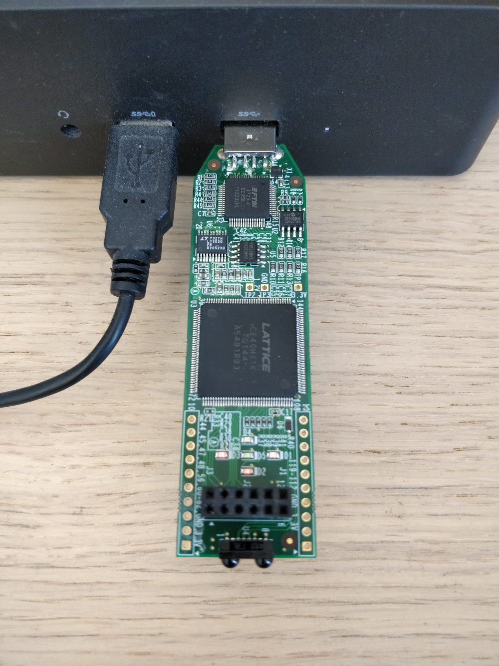
While iCE40 FPGAs are not the most capable FPGAs, they are cheap and – together with the Open Source tools – the ideal learning platform. If you are interested in the topic, I’d recommend Clifford’s recent talk at 35C3 about the state of the project. I had to try this out, so I bought a cheap iCEstick for around 25EUR. (I didn’t get the memo that the cool kids are now using the iCEBreaker board.)
I had no idea about FPGAs, but I found an excellent tutorial on GitHub. It is in Spanish but Google Translate can jump in here.
The general workflow of IceStorm, Clifford’s Open Source tools, is to write your design in Verilog and
- synthesize it with Yosys
- place and route with NextPNR
- create the bitstream with
icepack - copy the bitstream on the device with
iceprog
…no worries, a Makefile has you covered.
Pet Project: SPI Flash Reader
The iCEstick doesn’t have many peripherals to play with, so I decided to experiment with the onboard SPI flash. The goal was to read data from flash and send it to the PC through UART, i.e., serial line.
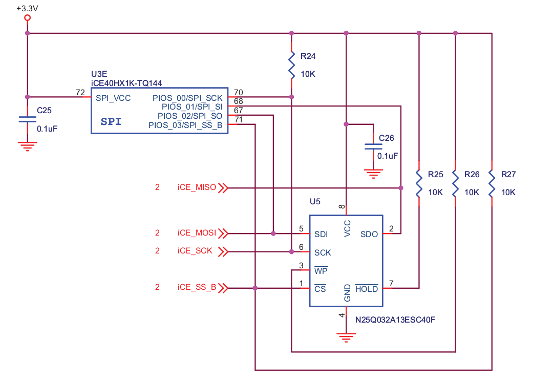
The schematics look a bit complicated, since there are three devices connected to the SPI bus. Obviously the FPGA and the flash controller but also the FTDI controller, which provides USB connectivity and is used for flashing the bitstream. The bitstream only needs about 32k of the 16Mb flash, so there is plenty of room.
I put a text file at 1M using iceprog:
iceprog -o 1M foo.txt
To access UART and the flash I needed some Verilog code. I didn’t start from scratch but used the UART transmitter from the tutorial and the SPI flash reader from Sylvain Munaut.
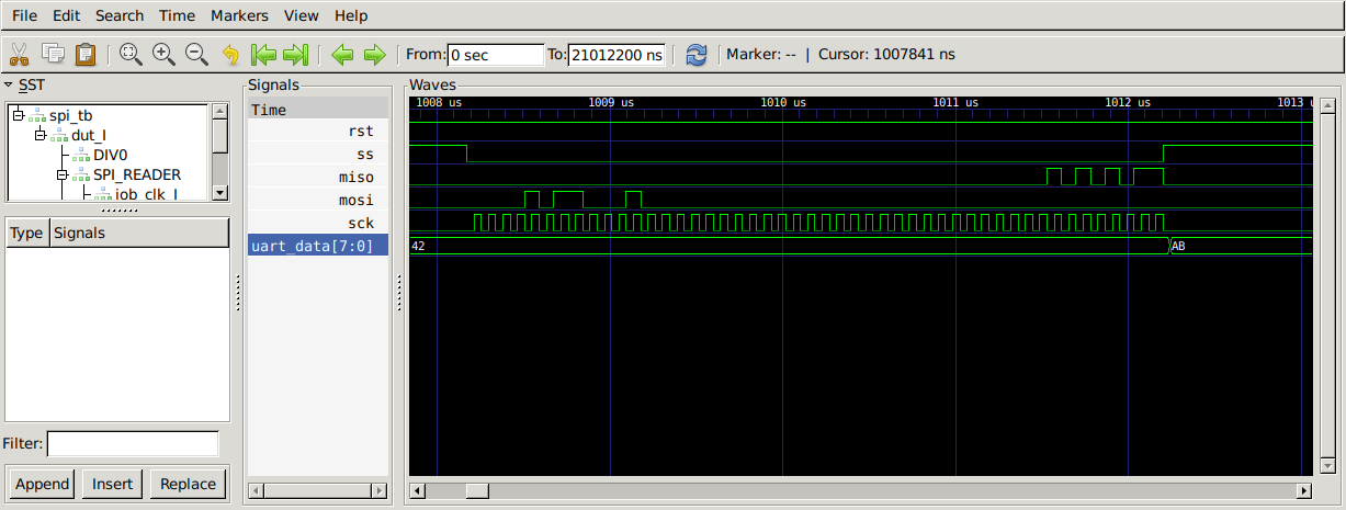
The main task was to puzzle everything together, setup simulations, and to check that the bus access looks like in the data sheet of the flash chip. I don’t want to go into the details here, but you can checkout my (probably embarrassing) code and Makefiles on GitHub.
One lesson learned is that my favorite way of debugging by staring at the code didn’t work all to well with FPGAs. I really needed a test bench to simulate the signal and data flow. I also simulated a reply from the flash controller (0xAB) and compared the signal with the ones in the data sheet of the flash controller.
The Verilog flash controller sends a read command without any setup.
However, by default, the SPI flash is put into deep sleep after the FPGA read the configuration.
In this mode, it would just ignore the read command.
To avoid this, one has to use the -s switch of icepack when generating the bitstream.
> icepack --help
[...]
  -s
      disable final deep-sleep SPI flash command after bitstream is loaded
The final step is to create a physical constraints file (a .pcf file) that maps the inputs and outputs of the final Verilog module to pins of the FPGA.
# clock
set_io clk  21
# UART
set_io tx    8
set_io ss   71
# SPI
set_io miso 68
set_io mosi 67
set_io sck  70
# LED
set_io D1 96
When this is done, you can a run terminal (like screen or GTKTerm) to connect to the serial output and watch the data that the FPGA reads from the flash and sends to the PC through.